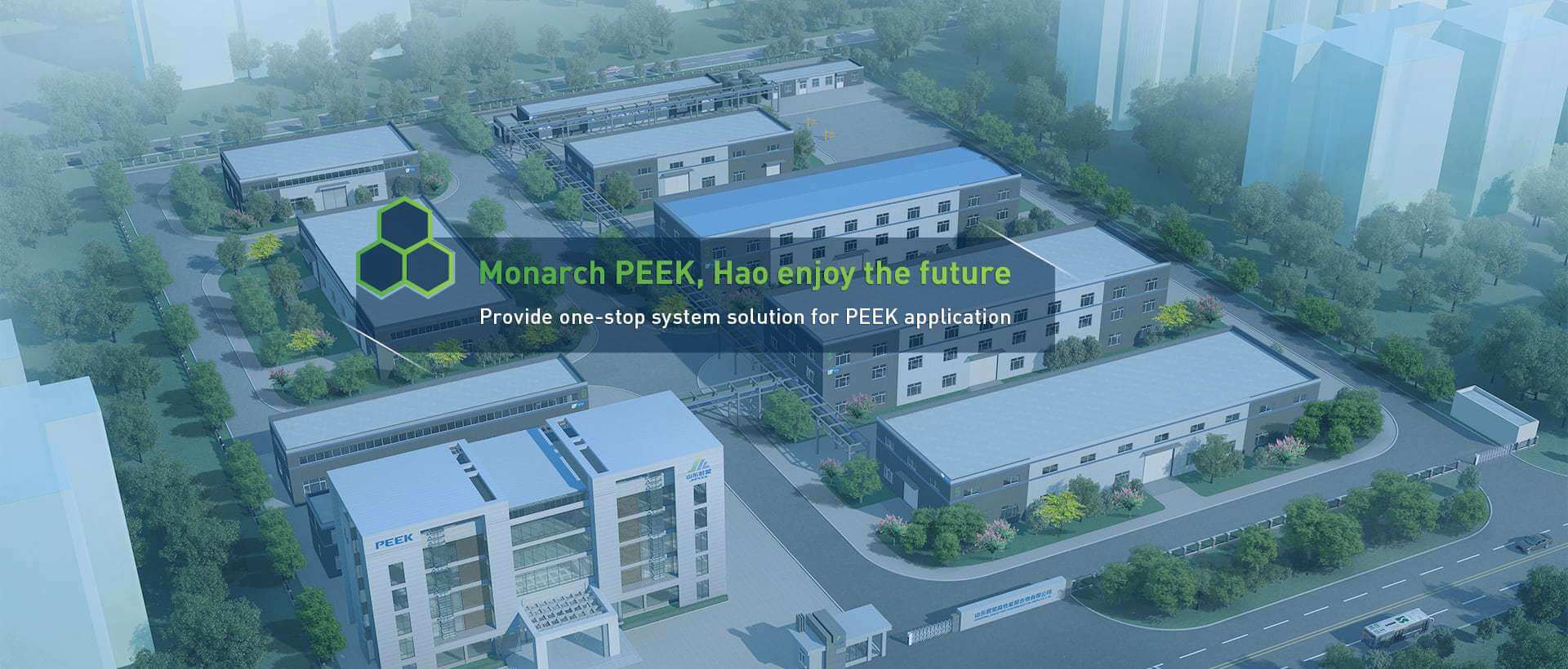
Shandong Junhao
Professional manufacturer of PEEK

No content yet

Explore the unique advantages that set us apart from the competition.
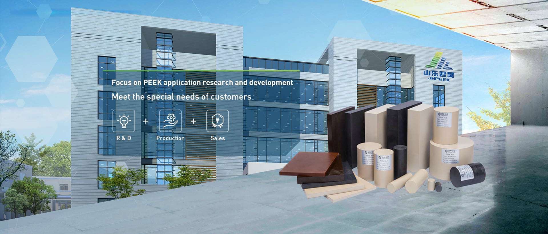
Junhao focuses on the research and development and production of high-performance polymers such as PEEK (polyetheretherketone), PI (polyimide), and PBI (polybenzimidazole).
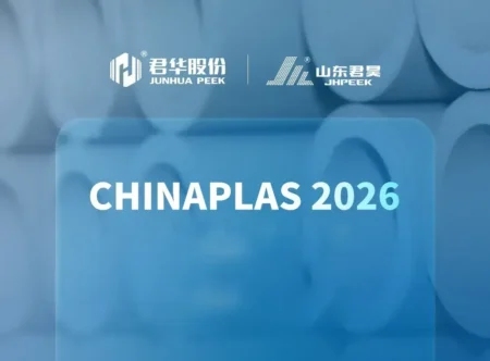
CHINAPLAS 2026 will grandly open on April 21, 2026, at the Shanghai National Exhibition and Convention Center. Junhua Group sincerely invites you to attend this…
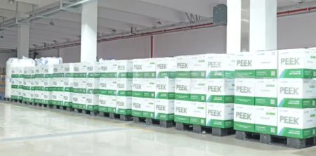
Shandong Junhao Resin Particles have been market-proven. Not only have we achieved stable batch deliveries, but we’ve also successfully launched ten tons of our products…
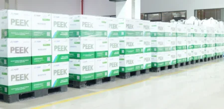
The new custom-designed packaging boxes for PEEK pellets developed by Shandong Junhao High-Performance Polymer Co., Ltd. have been completed and officially launched. Each new packaging…
Contact Us Now and Enjoy a One-Stop Solution!Fill the Form to Get a Quote, Product Manual, Performance Parameters, Custom Solutions, Technical Consultation, and Samples
We use cookies to improve your experience, conduct statistical analysis and provide personalized advertising. For more information, please refer to Cookie Statement
We use cookies to improve your experience, conduct statistical analysis and provide personalized advertising. For more information, please refer to Cookie Statement